Quick Turn Rigid Flex PCB Fabrication All In One Guide
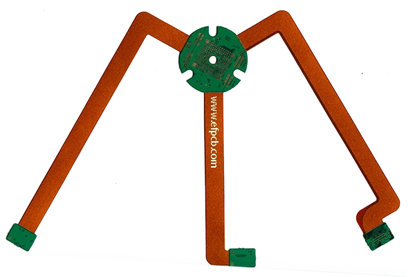
In a fast-paced electronics industry, prototyping and manufacturing complicated parts quickly can mean the difference between success and failure. This is particularly the case with rigid flex circuits, which are key enablers for high-end aerospace, medical devices, and consumer gadgets. This overview details out the important stages in the process of quick turn rigid flex PCB manufacturing that lead to maintaining speed with quality. The Rigid Flex PCB Fabrication Flow Rigid flex PCB manufacturing is a hybrid process that uses products of the rigid board and flexible board manufacturing processes to build the end product. The challenge is to bring together these diverse materials and techniques to create a single, enduring unit. In quick turn rigid flex PCB manufacturing, each step of the process has to be as sewed up as possible while still producing a viable product. Material Preparation and Inner Layer Imaging It all starts with materials selection. Typically the flexible sections have a polyimide core and the rigid areas are constructed with FR-4 epoxy. A layer of copper foil is laminated to these substrates. For rigid flex PCB manufacturing in a haste, these materials are just what you need. The inner layer circuit patterns are then formed by coating a photoresist, exposing it to UV light through a photomask, and developing it, then chemically etching the exposed copper layer. Lamination and Layer Bonding I’d say this is really the fundamental stage. The etched flexible layers are accurately registered to the rigid FR-4 layers and a bonding adhesive, typically a nonflow prepreg. The entire stack-up is then loaded into a lamination press. Under tremendous heat and pressure, the layers are bonded into a monolithic entity. The precision of this alignment and the controlled lamination cycle is critical for the success of quick turn rigid flex PCB fabrication. Drilling and Plating After bonding, vias, which are holes that serve as electrical connections from one layer to another, are drilled through the board. Mechanical drilling is still used for the rigid portions of the stack and laser drilling for the intricate features in the flexible sections. The board is then copper plated after drilling. This deposits a layer of copper inside drilled holes to create conductive pathway. This step is a bottleneck in many processes, so quick turn rigid flex PCB fabrication utilizes advanced plating chemistries and other solutions to minimize the impact.